QUAntum Technologies Experimental Platform
Local manager and PI: Andrea Salamon.
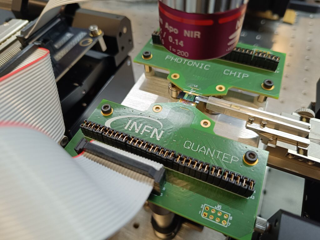
The main goal of the QUANTEP (QUAntum Technologies Experimental Platform) is the development of a common experimental platform for the study of optical quantum technologies on silicon photonics working at the 1550 nm telecom C-band.
In particular four main research lines will be investigated in the QUANTEP project:
- the design of silicon photonics circuits for Quantum Computing;
- the engineering of integrated Single Photon Sources;
- the development of integrated room temperature Single Photon Detectors;
- the use of Quantum Nanomaterials for integrated polarization control devices.
All the integrated circuits designed for the QUANTEP project will be implemented in a standard 220 nm Silicon On Insulator CMOS process, while all the special production process (e.g. ion implantations, nanowire or 2D materials depositions) will be performed in the research facilities of the QUANTEP team.
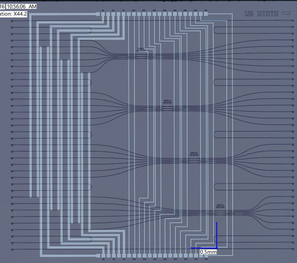
The study of linear optics Quantum Gates will be focused on the implementation and characterization of a two qubit Controlled-NOT (C-NOT) gate. This scheme makes use of linear, coincidence basis gate that performs all the operations of a controlled-NOT gate and requires only single photons at the input. This scheme could be a useful test-bed for the implementation of more sophisticated quantum circuits, which eventually will require on-chip single photon sources and detectors.
The quest for integrated Single Photon Sources will be performed through ion implantation with the aim to identify appealing classes of emitter centers in the telecom C-band. Ion implantation can unlock devices fabrication through the controlled placement of emitters registered to silicon photonic circuits. Such emerging technique involves both the delivery of individual impurities and their positioning with nm accuracy.
A room temperature Single Photon Detector, based on an integrated Bi2Se3/n-Si heterojunction will be developed. Bi2Se3 is part of a new class of materials called topological insulators with insulating or semiconducting properties in the bulk and nontrivial metallic Dirac fermions on the surface which are topologically protected. As a consequence, high charge mobility joined with bulk bandgap in the telecom range gives to these materials fast and sensitive characteristics suitable for single photon detectors.
Quantum Nanomaterials based on 2D materials and semiconductor nanowires will be used in the project to build nanodevices able to coherently and dynamically manipulate photon polarization by controlling the basic symmetries of the Hamiltonian of the quantum nanomaterial itself. Developed devices are expected to show tunable spectral range including the telecom bands, tunable optical response allowing for dynamical polarization control and on-chip connectivity with silicon photonics.